Samsung Electronics' Foundry Is Being Shunned: It Can’t Beat Either TSMC or SK Hynix

As one of the youngest members of the team, Tyler Hansbrough is a rising star in financial journalism. His fresh perspective and analytical approach bring a modern edge to business reporting. Whether he’s covering stock market trends or dissecting corporate earnings, his sharp insights resonate with the new generation of investors.
Authored On
Modified
Jensen Huang: "No Packaging Alternative Besides TSMC"
No Mention of Samsung Electronics’ HBM
Beyond Mature Nodes, Core Semiconductor Competitiveness Must Be Secured
In the global semiconductor arena, where innovation moves at breakneck speed and leadership is both hard-earned and easily lost, Samsung Electronics finds itself at a crossroads. Once heralded as a formidable force in chip manufacturing, Samsung’s foundry business now faces a stark reality—being overlooked by the very partners who once counted on its capabilities. The most recent blow came from none other than NVIDIA CEO Jensen Huang, whose comments and actions during a series of high-profile industry events in Taipei have sent ripples through the tech world. While competitors TSMC and SK Hynix were lauded, Samsung received what can only be described as a cold shoulder—raising questions about the future direction of its semiconductor strategy.
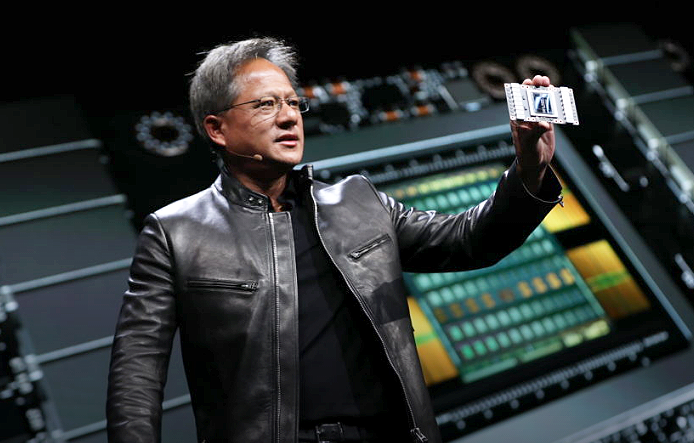
Jensen Huang Draws a Line: Favoring TSMC and SK Hynix Over Samsung
At the GTC Taipei global press conference on May 21, held at the prestigious Mandarin Oriental Hotel, Jensen Huang was asked about the role of advanced packaging technologies in the evolution of artificial intelligence (AI). In response, he held up one of NVIDIA’s latest chips and remarked, “Look at the size of our chips—this is how small they are.” He went on to explain that such miniaturization and performance were made possible through TSMC’s proprietary Chip-on-Wafer-on-Substrate (CoWoS) technology. This method places multiple chips tightly together on a wafer and then bonds them onto a substrate, drastically shortening signal travel distances and thereby increasing data transfer speed and efficiency.
CoWoS, which is central to integrating GPUs and High Bandwidth Memory (HBM) in AI accelerators, has become indispensable for NVIDIA’s product architecture. When a reporter asked about Samsung's advanced packaging capabilities as an alternative, Huang gave a pointed reply: “CoWoS is a highly advanced technology at this point,” adding unequivocally, “Right now, there are no other options besides CoWoS that NVIDIA can use.” His statement made it clear—Samsung is not even under consideration.
The rationale behind this technological allegiance is rooted in the limitations of Moore’s Law. As Huang explained, the once-reliable trend of doubling transistor density every 24 months has stalled. The number of transistors that can be effectively packed into a single die has plateaued, forcing companies to adopt chiplet-based architectures. TSMC’s CoWoS is currently unmatched in enabling this transition.
But Huang’s disapproval of Samsung did not end with packaging. In the HBM sector—a key battleground for AI chip supremacy—Samsung was again bypassed. The industry had anticipated a favorable signal from Huang regarding Samsung’s long-awaited HBM3E memory. After all, nearly a year had passed since the company underwent qualification tests to supply these chips to NVIDIA. Yet, during his public appearances, Huang mentioned Samsung only once—and that in passing—when discussing a 6G AI technology partner.
In stark contrast, he showcased deep alignment with SK Hynix. On May 20, Huang visited SK Hynix’s booth at Computex 2025, Asia’s largest IT and computing trade show. There, he offered public praise for their HBM4 (6th generation) chips and even left cheerful handwritten notes: “I love SK Hynix” and “One Team.” This display of enthusiasm followed SK Hynix’s successful delivery of HBM4 samples to NVIDIA back in March, with full-scale mass production slated for the second half of the year. It was a symbolic gesture, but one with strategic weight—highlighting where NVIDIA’s trust and future investments lie.
Mature Process Demand Offers Temporary Relief
Despite these blows in next-generation technologies, Samsung has not been entirely marginalized in the foundry market. The company is experiencing surging demand in mature nodes, particularly in the 5nm and 8nm categories, which continue to play a significant role in consumer electronics and enterprise applications.
A notable example is Samsung’s win in securing the production of NVIDIA’s Tegra system-on-chip (SoC) for the upcoming Nintendo Switch 2 console. Nintendo had originally weighed the merits of Samsung’s 5nm and 8nm options. In the end, the 8nm process won out, primarily due to its cost advantages and higher production yield. This node does not rely on extreme ultraviolet (EUV) lithography—a technology that, while powerful, is also expensive and more complex to implement.
Samsung’s influence extends beyond gaming. The company’s foundry has also clinched deals with global clients like IBM, which entrusted Samsung with the production of its Telum 2 mainframe processor and Sapphire AI accelerator. These chips—unveiled at the Hot Chips 2024 conference—are integral to IBM’s next-generation Z Series enterprise server systems, and are being manufactured using Samsung’s 5nm technology.
Looking to the future, Samsung aims to leverage its 5nm capabilities in the automotive sector. Beginning in 2030, the company plans to manufacture semiconductors for Advanced Driver Assistance Systems (ADAS) in Hyundai’s luxury Genesis line. These chips will play a critical role in enhancing vehicle safety, automation, and driver experience.
While these contracts are promising, they serve more as financial lifelines than indicators of future leadership. The revenues generated from mature process nodes help Samsung stay afloat, but they do not position the company at the cutting edge of semiconductor innovation.
The Real Race: 2nm Nodes and HBM Supremacy
The challenge for Samsung is clear. Market dominance in semiconductors will be decided not by mature processes but by who leads the charge in 2nm manufacturing and high-performance memory for AI systems. These are the frontlines of the next era in chip technology—and the areas where Samsung is currently trailing.
Industry experts caution that the situation is urgent. “Chinese foundries with aggressive pricing are quickly catching up in mature process segments,” warned one market analyst. “Samsung’s position in the 5nm and 8nm market could gradually erode.” He stressed that Samsung must not only defend its current territory but also make aggressive moves into future battlegrounds.
To do so, Samsung must first achieve a critical milestone—passing NVIDIA’s qualification tests for HBM3E. At the annual shareholders’ meeting in March, Jun Young-Hyun, head of the company’s Device Solutions (DS) division, assured investors that Samsung’s 12-layer HBM3E products would enter market leadership “as early as the second quarter, or by the second half of the year at the latest.” Yet, with the third quarter fast approaching, there is still no confirmation that the qualification has been completed.
Samsung is now caught in a race against time. The company must translate its gains in mature nodes into a solid foundation for long-term innovation. Only by accelerating its development in 2nm technologies and reclaiming relevance in HBM can Samsung hope to win back key partners—and reassert itself as a leader in the semiconductor world.
As one of the youngest members of the team, Tyler Hansbrough is a rising star in financial journalism. His fresh perspective and analytical approach bring a modern edge to business reporting. Whether he’s covering stock market trends or dissecting corporate earnings, his sharp insights resonate with the new generation of investors.
Similar Post