TSMC to Drastically Expand 2nm Production Capacity, Undermining Samsung’s Pursuit

Authored On
Modified
TSMC to Supply 100,000 Wafers per Month by Late 2026
Secures Key Clients Including Apple and Nvidia
Confident in Yield and Ecosystem Superiority Amid Samsung’s Aggressive Catch-Up
The battle for supremacy in the global semiconductor supply chain is intensifying, with the race toward 2-nanometer (nm) chip production emerging as the next critical frontier. While Samsung Electronics is aggressively entering the 2nm foundry market, even at the cost of steep operating losses, TSMC has unveiled a bold capacity expansion strategy that threatens to neutralize Samsung’s pursuit. Industry analysts warn that if TSMC not only retains its lead in yield but also absorbs a significant share of production volume, Samsung’s strategic catch-up effort could be structurally thwarted.
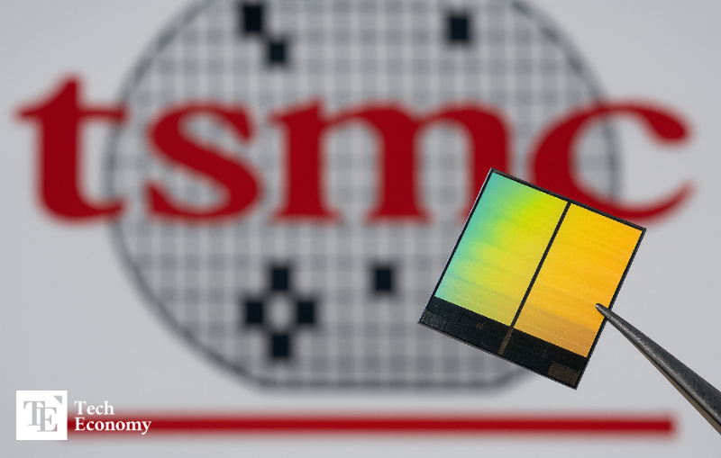
TSMC Accelerates 2nm Investment
According to WCCFTech and other foreign media outlets on August 4 (local time), TSMC is significantly expanding its production capabilities to address the anticipated boom in the 2nm chipset market starting in 2026. Having already begun taking orders as early as April, TSMC is accelerating its infrastructure buildout as major fabless customers—Apple, Qualcomm, MediaTek—alongside global AI platform giants such as Nvidia, AMD, Google, Amazon Web Services (AWS), and OpenAI, scramble to secure early production slots.
Currently, TSMC is constructing a total of four 2nm fabrication plants in Taiwan’s southern city of Kaohsiung and the northern science park of Baoshan, Hsinchu. The P1 fab in Kaohsiung is already mass-producing at a rate of 10,000 wafers per month. The adjacent P2 fab, still in the equipment installation phase, is expected to begin trial production within three to four months, eventually ramping up to 30,000 wafers per month. The plant expansion, initiated in late March, entered equipment installation by early August—a highly unusual turnaround, as advanced fab and cleanroom construction typically require at least four months, with an additional four months for equipment setup and testing.
In Hsinchu, Taiwan’s semiconductor hub, 2nm conversion is also progressing rapidly. Trial production has been completed at the P1 fab, with mass production imminent, while the P2 fab is currently assembling its production lines. TSMC's 2nm production output is expected to start at 40,000 to 50,000 wafers per month in the second half of this year, reaching 53,000 wafers in early 2026 and 60,000 wafers by mid-2026. TSMC asserts that it has already secured stable yields in the trial phase, effectively completing its mass production readiness.
Furthermore, TSMC is considering establishing three additional fabs in Kaohsiung for next-generation processes, including 2nm and the A16 node (equivalent to 1.6nm). Taiwan’s Liberty Times reported that surging demand for AI semiconductors has already driven 2nm orders beyond those for 3nm and 5nm nodes.
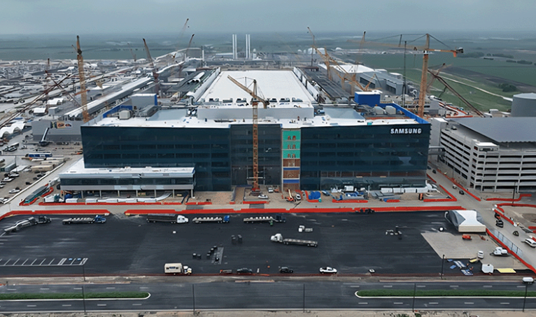
Samsung Bets the Future of Its Foundry on 2nm
Samsung Electronics is also moving toward mass production of 2nm semiconductors. On August 1, during its SAFE Forum 2025—an industry event for foundry partners—Samsung announced a revised roadmap, delaying its 1.4nm mass production target from 2027 to 2029. In exchange, the company plans to refine its 2nm process, set for mass production later this year, to improve fab utilization and profitability. To that end, it is expediting the buildout of production lines at its new foundry fab in Taylor, Texas. Although originally scheduled for early next year, the investment is now being fast-tracked for execution by the end of this year.
Given the company’s current struggles to secure its own smartphone chip orders, the success of its 2nm process has become a matter of urgency. Samsung’s poor yields in sub-3nm nodes have already led to massive foundry losses and a migration of major clients to TSMC. As a result, Samsung is opting to deliver partial volumes to clients even before achieving stable yields—judging that this approach, despite short-term losses, is more advantageous than waiting indefinitely.
Samsung’s semiconductor division is targeting the first half of next year to deploy its in-house designed and manufactured 2nm-based Exynos chips in the Galaxy S26 series. The competitiveness of these chips is expected to serve as a critical turning point. A semiconductor industry insider noted, “Samsung has long prioritized node leadership at the expense of process maturity, leading to low yields and eroded client trust. This renewed focus on stability is a positive development.”
70% Yield the Break-Even Threshold
To gain a foothold in the 2nm foundry market, Samsung is leveraging its proprietary GAA (Gate-All-Around) technology. The recent $16.5 billion contract with Tesla is seen as a potential sign of restored market confidence in Samsung’s GAA-based offerings. The company plans to manufacture the AI6 semiconductor—central to Tesla’s autonomous driving systems—using its 2nm process.
The AI6 chip is a core component for realizing Tesla’s Full Self-Driving (FSD) vision. As a second-generation advancement over the AI4 chip currently deployed in Tesla’s robotaxi business, the AI6 is expected to deliver more than twice the performance of the AI5 chip, which is scheduled for mass production later this year. The AI6 will likely be deployed in humanoid robots and supercomputers, positioning it as Tesla’s central processing platform across all business domains. Tesla CEO Elon Musk hinted at broader applications when he stated on his X (formerly Twitter) account that "$16.5 billion is just the minimum, and actual production volume could be several times higher.”
Previously, Samsung supplied Tesla with the AI4 chip produced on a 7nm process. However, the AI5 chip—manufactured on a 3nm node—was sourced from TSMC. Industry sources suggest that Samsung regained Tesla’s business primarily due to its lower pricing. Still, this contract may not be profitable for Samsung. To secure the deal, the company likely undercut TSMC’s pricing, and it still faces yield challenges that undermine margins. Moreover, TSMC's production capacity is currently maxed out, limiting its ability to handle high-volume orders. Samsung’s Texas fab, located in proximity to Tesla’s headquarters, is well-positioned to meet volume demands while aligning with the Trump administration’s push for "Made in America" production.
Nevertheless, some industry voices warn that unless Samsung dramatically improves its yields, the Tesla deal could become a liability. Samsung’s current 2nm yields are not yet at break-even levels. While estimates vary, industry observers suggest that initial yields were below 30% but have since risen to the 40–50% range. Some projections even suggest a yield nearing 60%.
The general consensus is that a 70% yield is the minimum threshold for profitability. In comparison, TSMC is reportedly achieving yields of over 90% on its 2nm process. This underlines TSMC’s continued edge in both production maturity and customer ecosystem strength. TSMC’s 2nm strategy can be summed up as one of “ultra-gap technology,” “massive production capacity,” and a “premium pricing model.” The company is scaling up production at a pace four times faster than the transition from 5nm to 3nm, solidifying its position at the heart of the global advanced semiconductor supply chain. Most analysts agree that unless competitors can achieve a dramatic leap in pricing or capacity, TSMC’s near-monopoly is likely to endure.
Similar Post