Samsung Electronics Sets Up New Packaging Research Center in Japan to Stay Ahead of Taiwan

Authored On
Modified
Samsung Electronics to invest $172 million in a new research center in Yokohama, Japan
Strengthening advanced semiconductor “packaging” capabilities for next-generation chips
Korea’s packaging technology still trails behind Taiwan’s cutting-edge leadership
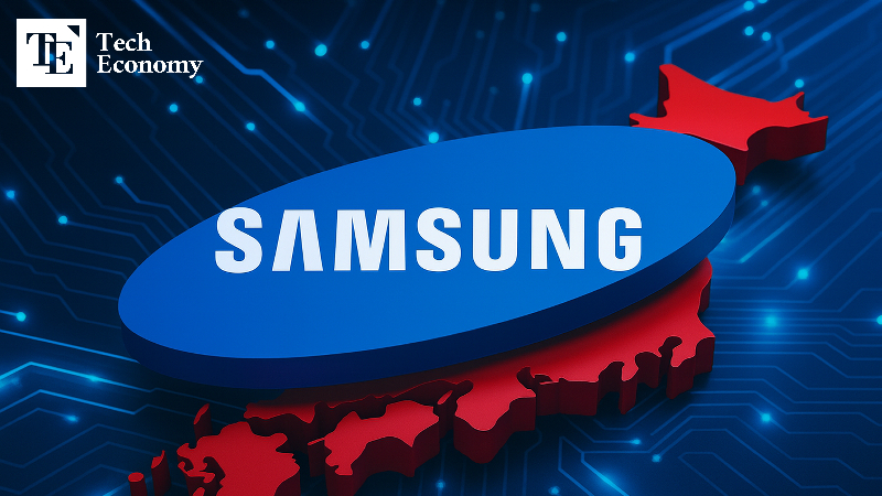
Samsung Electronics will establish a state-of-the-art packaging research center in Yokohama, Japan. As packaging technology emerges as a key weapon in the global semiconductor power race, the company plans to join forces with Japan’s academic and industrial sectors to bolster its competitiveness. The market is now watching closely to see whether this new facility will enable Samsung to stand shoulder to shoulder with established leaders such as Taiwan’s TSMC and ASE.
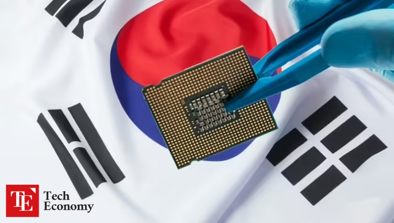
Samsung Electronics Secures New R&D Base in Japan
According to the semiconductor industry on August 14, the Device Solutions (DS) division of Samsung Electronics’ Japanese subsidiary will invest ¥25 billion (approximately $172 million) to establish an advanced packaging research center in Yokohama. This move gives concrete shape to the packaging investment plan the company announced in December 2023. Operations are slated to begin in March 2027, with local research staff to be recruited in the lead-up. Yokohama City has designated Samsung as a “Certified Business under the Corporate Location Promotion Ordinance” and will provide a subsidy of ¥2.5 billion (about $17 million).
Samsung has purchased the “Leaf Minato Mirai” building, located in the heart of Yokohama’s Minato Mirai 21 district, with a total floor area of 47,710㎡ (14,332 pyeong; 12 floors above ground, 4 below). Part of the space will house the new packaging research center and pilot production facilities. This marks the first time in 10 years that Samsung will own a large-scale building in Japan, following the sale of its 57% stake in the Roppongi headquarters building of Samsung Japan in March 2015 as part of restructuring efforts.
The decision to set up the packaging research center in Japan stems from a focus on technology collaboration. Samsung plans to enhance its advanced packaging capabilities through partnerships with the University of Tokyo, as well as Japanese materials, components, and equipment companies such as Disco (equipment), Namics (materials), and Rasonac (materials). TSMC took a similar approach in 2019, establishing a research center at the University of Tokyo to advance its own packaging technologies.
Japan’s “Alliance” Strategy in Semiconductor Packaging
Market watchers say Samsung Electronics has chosen the right timing for its investment, as the importance of back-end processes—particularly packaging—has grown sharply in recent years. In the past, semiconductor performance improvements were driven mainly by shrinking circuit linewidths in the front-end process. But with linewidths now below 10 nanometers, further scaling has become technically challenging. Back-end processes are gaining attention as they can enhance chip performance without reducing linewidths. Among these, advanced technologies such as 2.5D and 3D packaging and chiplets are considered the flagship solutions.
In response, Japanese OSAT (outsourced semiconductor assembly and test) companies have begun joining forces to boost competitiveness. In April, they formed the J-OSAT Association, bringing together about 30 member companies for formal collaboration. Nikkei Asia reported that before J-OSAT’s creation, there was no platform for information sharing, and with 80% of companies in Japan’s back-end sector being small and mid-sized enterprises, even basic industry data was not widely known. Now it is clear that Japan’s back-end production capacity exceeds 1.1 billion units per month, with output split roughly into 40% automotive, 40% industrial machinery, and 20% consumer products.
J-OSAT plans to focus on five key areas: automation, production data sharing, workforce development, and other strategic initiatives. It is also considering requesting subsidies from the Japanese government to acquire high-performance equipment. Makoto Sumita, J-OSAT’s inaugural chairman, noted that while front-end semiconductor processes require around ¥1 trillion (about $6.9 billion) in investment, much can be achieved in the back-end with just ¥10 billion ($69 million) to ¥20 billion ($138 million). He also claimed that adopting state-of-the-art equipment could cut production costs by as much as 20%.
“How Can Korea Beat Taiwan?” — Falling Behind in the Race
While Japanese packaging companies are leveraging collaborative structures to aggressively target the market, Korean firms remain largely absent, having failed to break into a segment dominated by Taiwanese players. Recently, TSMC has expanded its business from foundry into advanced packaging, building on its core manufacturing strength. According to Counterpoint Research, TSMC’s combined market share in foundry, packaging, and testing rose from 29.4% in Q1 2024 to 35.3% in Q1 2025. This surge is attributed to the company handling both the foundry and advanced packaging processes needed to pair SK hynix’s high-bandwidth memory (HBM) with Nvidia’s graphics processing units (GPUs) for AI accelerators. Taiwan’s ASE, a traditional packaging leader, also posted a 6.2% share in Q1, ranking third globally after Intel’s 6.5%.
In contrast, Samsung Electronics—Korea’s flagship player—held just 5.9% of the combined foundry, packaging, and testing market as of Q1. Looking solely at the packaging sector, no Korean company ranks in the global top 10. An industry insider remarked, “Korea lags behind Taiwan and the U.S. in advanced packaging, and in general-purpose packaging—where it has some competitiveness—it is being chased by Malaysia and China. For a country calling itself a semiconductor powerhouse, our domestic ecosystem is surprisingly weak.”
As Korea continues to struggle in the packaging power race, Samsung has sought to emulate TSMC’s model by offering a turnkey service that bundles both foundry and advanced packaging for clients. However, results have been limited so far, with Samsung still trailing TSMC in both capacity and technical capabilities for advanced packaging. The establishment of the new packaging research center in Japan is seen as a strategic move to overcome these shortcomings.
Similar Post