Samsung Secures IBM CPU Orders, Strengthens Foothold With Mature Nodes Against TSMC

Authored On
Modified
Samsung Wins IBM CPU Orders With Upgraded 7nm Foundry Process
Nintendo Switch 2 SoC to Be Built on Mature 5nm Node
Tesla Deal on 4nm Seen as Stepping Stone Toward Advanced Process Leadership
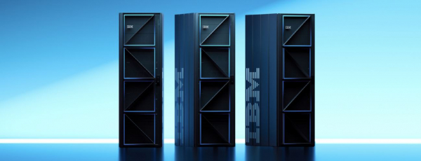
Samsung has reportedly secured a foundry contract to produce IBM’s next-generation data center chip, the Power11. While the technology gap with rival TSMC in leading-edge processes remains difficult to close, Samsung is instead focusing on strengthening its position in mature nodes by winning key clients—an approach seen as shoring up its foundations.
Leveraging 7LPP to Secure IBM as a Client
According to industry reports on the 19th, Samsung Electronics’ foundry division will manufacture IBM’s next-generation server CPU, the Power11, using its upgraded 7-nanometer process, known as 7LPP. This node was the first in the world to apply EUV (extreme ultraviolet) lithography, enabling more precise and finer circuit patterns. Compared with the previous generation, the 7LPP process delivers a 23% performance boost and a 45% reduction in power consumption, significantly improving overall efficiency.
In collaboration with IBM, Samsung also plans to apply its advanced “2.5D ISC architecture packaging” technology to further maximize chip performance. This packaging method, widely used in high-performance semiconductors, places multiple dies close together within a single package to achieve faster data transfer rates.
The IBM Power11, which Samsung will produce, is designed to deliver 99.9999% data center uptime, allowing system maintenance without downtime. Its standout feature is high power efficiency. The chip is also equipped with post-quantum cryptography certified by the U.S. National Institute of Standards and Technology (NIST). This provides strong protection against harvest-now, decrypt-later attacks and firmware integrity threats, ensuring enhanced system security.
Nintendo Secured Through Mature Node Strategy
Analysts note that Samsung has been building its foundry order book this year largely on mature processes. In May, industry reports revealed that Samsung would manufacture Nvidia’s Tegra system-on-chip (SoC) for Nintendo’s highly anticipated Switch 2 using its 8nm node. Nintendo had considered both Samsung’s 5nm and 8nm processes but ultimately chose the latter—without EUV lithography—due to cost and yield advantages.
The Switch 2, powered by Samsung’s SoC, went on to achieve explosive success in the market. Within 24 hours of launch, it sold over 3 million units, setting a new record. By contrast, the original Switch sold 2.7 million units in its first month. Nintendo has set a shipment target of 20 million units for fiscal 2026 (April 2025–March 2026). Both Bloomberg and Japanese consultancy Kantan Games forecast 20 million sales in the first year, while research firm Omdia expects 14.4 million units to be sold by the end of this year.
The Switch 2 boom is a clear boost for Samsung Foundry, which has struggled with declining utilization rates. A market insider commented: “Securing orders for the Switch 2 is significant in itself, and Nintendo may also turn to Samsung’s other processes for performance upgrades after launch. If this deal becomes a strong reference for game console production, Samsung could attract future orders from competitors such as AMD.”
Samsung’s Strategy: Exploiting TSMC’s Blind Spots
In July, Samsung Foundry won a major contract with Tesla for artificial intelligence (AI) chips. On July 28, Samsung disclosed that it had signed a $16.5 billion foundry supply agreement with a global company—later revealed to be Tesla. Under the deal, Samsung will manufacture Tesla’s next-generation AI chip, the AI6. After the announcement, Tesla CEO Elon Musk highlighted the partnership on social media and hinted that the AI6 project could pave the way for broader collaboration between the two companies.
Following the Tesla contract, Samsung reportedly secured multiple additional clients. With few companies besides Samsung capable of competing with TSMC in advanced foundry technology, landing Tesla as a flagship customer significantly boosted market confidence. An industry insider noted: “Samsung has signed a number of small- to mid-scale foundry deals in the second half. While none are on Tesla’s scale, more mid-tier fabless firms and AI startups, both in Korea and abroad, are choosing Samsung for chip production.”
Samsung’s focus on nodes at 4nm and above, rather than chasing the cutting-edge 2nm or 3nm, is seen as a deliberate strategy to exploit TSMC’s “blind spots.” Since catching up to TSMC in leading-edge processes remains difficult in the near term, Samsung is instead diversifying its client base in mature nodes where TSMC’s dominance is less overwhelming. TSMC has already pushed trial yields for its 2nm process above 60%, with mass production expected to reach as high as 90%. In contrast, early trial yields for Samsung’s Exynos 2600 reportedly remain around 30%, underscoring the challenge of competing head-on in the most advanced nodes.
Similar Post