Hybrid Bonding is Essential for the 'HBM 16-Stack Era'; Equipment Supply Chain Reorganization is Imminent

With a decade of experience in education journalism, Lauren Robinson leads The EduTimes with a sharp editorial eye and a passion for academic integrity. She specializes in higher education policy, admissions trends, and the evolving landscape of online learning. A firm believer in the power of data-driven reporting, she ensures that every story published is both insightful and impactful.
Authored On
Modified
HDB: An Essential Technology for HBM4 Commercialization
Optimistic Outlook with Advances in Precision Technology
But for Equipment Firms, a Profitable Business Model Is Still a Long Way Off
As demand for high-performance computing and artificial intelligence intensifies, high-bandwidth memory (HBM) is taking center stage in the semiconductor world. In this rapidly evolving landscape, hybrid bonding (HDB) has emerged as the next critical step in pushing HBM beyond its current limitations. At the forefront of this transformation are Samsung Electronics and SK Hynix, both accelerating investments in HDB technology to meet the growing need for denser, faster, and more power-efficient memory. But as the industry embraces this next-generation packaging innovation, it also stands on the brink of a profound restructuring — particularly in the semiconductor equipment supply chain.
While HDB promises performance breakthroughs and architectural advantages, industry insiders warn that the benefits may not be equally shared. In particular, smaller equipment manufacturers are raising concerns about profitability and bargaining power in a market increasingly controlled by tech giants.
Overcoming Barriers: The Rise of Hybrid Bonding
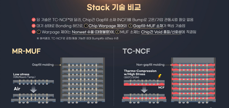
The introduction of HDB technology is not just a shift — it’s a response to the very real physical and engineering limits of existing HBM production methods. For Samsung, the traditional TC-NCF (Thermo-Compression Non-Conductive Film) process has been the backbone of HBM manufacturing. This method inserts ultra-thin insulating films between stacked DRAM chips and compresses them with heat, effectively filling inter-chip voids and preventing warpage. However, ensuring uniform heat and pressure across more than a thousand micro bumps is technically challenging. The result has been a relatively high defect rate, despite the method’s structural advantages.
SK Hynix took a different path with the MR-MUF (Molded Reflow-Mold Underfill) process. This approach involves stacking and soldering chips in bulk inside high-temperature ovens, then injecting a sticky liquid underfill between soldered layers. The process minimizes thermal damage to chips, but it struggles with scaling down inter-chip spacing, making it less viable for ultra-dense stacking needed in future HBM designs.
Hybrid bonding was developed as a solution to these issues. Unlike previous techniques that rely on films or liquids, HDB uses only solid-state materials — insulators and conductive metals like copper — to bond chips. This enables tighter stacking with increased electrical performance, improved thermal management, and the potential to recover over 80 micrometers of usable space between chips. These advantages have earned HDB the label of a "dream packaging technology" in the industry.
Yet for years, commercialization of hybrid bonding remained a distant goal due to the complexity of bonding dissimilar materials within a single wafer without adhesives. That changed in 2024, when Samsung and SK Hynix initiated substantial investments in HDB-capable infrastructure. What was once considered experimental is now a strategic necessity. Industry experts now believe that HDB is no longer just a trend — it has become a minimum entry requirement for future participation in the HBM market, particularly starting with HBM4 and HBM4E, which are planned for production by Samsung and SK Hynix respectively.
As one expert in the field noted, this is a defining moment in memory packaging. The evolution of HBM technology has reached a point where even the basic semiconductor architecture is being redesigned to overcome the miniaturization limits of traditional bonding methods.
Disrupting the Equipment Landscape: New Opportunities and Old Challenges
The ripple effect of hybrid bonding adoption is being felt most acutely in the semiconductor equipment ecosystem. With HDB expected to become the dominant technique for next-generation HBM stacking, the equipment supply chain is undergoing a dramatic shift. The intricate requirements of HDB — including sub-micron alignment, precision compression, and plasma activation — demand a far higher level of complexity than legacy processes.
Historically, the supply of critical equipment for HBM processes has been dominated by a few major players, including U.S.-based Applied Materials (AMAT) and Japan’s Tokyo Electron (TEL). But that dominance is beginning to erode.
Samsung, in particular, has been actively reshaping its supplier landscape. In June 2023, the company published a technical study on “D2W Hybrid Cu Bonding Technology for HBM Stacking,” revealing that stacking up to 17 chips within a 775µm form factor would require minimizing spacing through Hybrid Copper Bonding (HCB). Using equipment developed by SEMES, Samsung successfully fabricated a 16-layer HBM3 sample, which functioned normally. This achievement marked a deliberate departure from its dependency on traditional foreign suppliers, signaling a new era of collaboration with mid-sized equipment firms in both South Korea and abroad.
SK Hynix is following a similar path. For years, it relied exclusively on Hanmi Semiconductor for HBM manufacturing equipment. However, in a move that broke this exclusivity, SK Hynix recently signed a ₩42 billion ($30 million) supply deal with Hanwha Semitek, disrupting the long-standing monopoly. As the global HBM market leader, SK Hynix now views the development of a diversified vendor base as crucial to maintaining competitiveness and ensuring a robust, flexible production pipeline.
Still, not all participants in the supply chain are benefitting equally. Smaller Korean equipment companies, despite their role in enabling this technological leap, often lack the bargaining power to negotiate favorable terms. One executive from a domestic equipment supplier shared that while their firm delivers top-tier technology to major clients like Samsung and SK Hynix, they have almost no leverage to raise unit prices or renegotiate supply conditions. In effect, these companies are playing an indispensable role in a system where profits remain elusive, even for technically superior suppliers.
Worse still, as customization demands grow — particularly for HDB-specific adaptations — the risk of under-recovered investments increases. The same executive explained that many small equipment firms are now absorbing the burden of costly R&D with no guaranteed return, making it increasingly difficult to justify participation in what is otherwise a booming sector.
Samsung’s Strategic Comeback and the Uneven Playing Field
Samsung’s push for hybrid bonding is about more than just keeping pace — it’s a bold attempt to reclaim leadership in the HBM sector. The company has lost ground in recent years, but it now sees HDB as the key to a dramatic turnaround.
In February 2025, Samsung installed hybrid bonding equipment at its Hwaseong facility in Gyeonggi Province and hosted a high-profile ceremony to underscore the significance of the move. Speaking at the event, Song Jae-Hyuk, Chief Technology Officer of the Device Solutions division, described the company’s position through a sports analogy. It was as if Samsung had led the game until the ninth inning, only to lose the lead — and now, entering the bottom of the ninth, the first step to victory was getting the leadoff runner on base. Implicit in his message was the belief that HDB would be the decisive catalyst for a comeback.
But as Samsung charges forward, many in the equipment sector are left to grapple with the uncomfortable reality that technological advancement does not guarantee equitable gains. The current structure of the market leaves smaller vendors in a bind — vital to innovation, yet excluded from the pricing power that defines profitability. Despite their contributions, they continue to navigate a system where the giants dictate the terms.
As the industry steps into the HBM 16-stack era, hybrid bonding is clearly the way forward. It offers a solution to long-standing engineering problems, unlocks new packaging efficiencies, and aligns with the future needs of AI and high-speed computing. But this progress comes with growing pains. Whether the benefits of this transformation will extend beyond the largest players — and empower the broader semiconductor ecosystem — remains one of the most pressing questions facing the industry today.
With a decade of experience in education journalism, Lauren Robinson leads The EduTimes with a sharp editorial eye and a passion for academic integrity. She specializes in higher education policy, admissions trends, and the evolving landscape of online learning. A firm believer in the power of data-driven reporting, she ensures that every story published is both insightful and impactful.
Similar Post