Huawei Chipset Stuck at 7nm: Has the 5nm Barrier Hit a Wall?
Input
Modified
Huawei Faces Production Issues with Next-Gen 5nm AP
EUV Equipment Shortage Leads to Yield Around 30%
Production to Rely on Improved SMIC 7nm Process

As Huawei prepares to launch its next-generation smartphone, the Mate 80, later this year, industry insiders are projecting that its application processor (AP)—the "brain" of the smartphone—will be produced using a 7-nanometer (nm) process rather than the anticipated 5nm technology. Due to U.S. export restrictions on cutting-edge semiconductor manufacturing equipment like extreme ultraviolet (EUV) lithography machines, Huawei, in collaboration with China’s leading foundry SMIC, has pursued advanced manufacturing capabilities but appears to have encountered setbacks in mass-producing 5nm chips.
Kirin 9030 to Be Mass-Produced Using 7nm
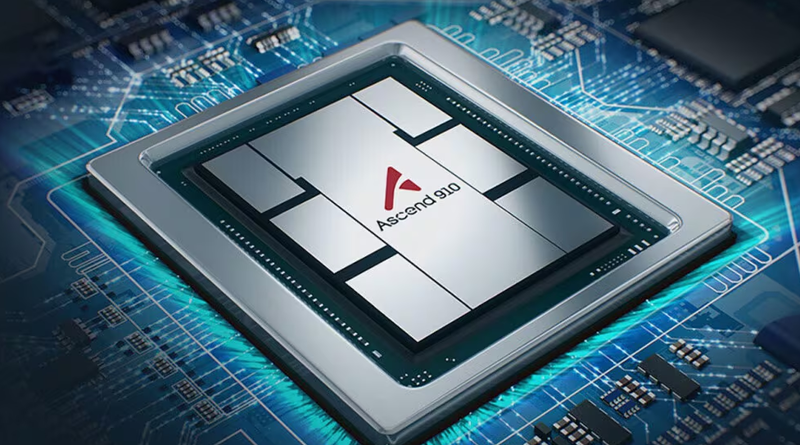
According to the semiconductor industry on July 10, the Kirin 9030 chipset, expected to power Huawei’s Mate 80, is likely to be manufactured using SMIC’s 7nm process. Huawei has reportedly improved the design and process to boost the Kirin 9030’s overall performance by about 20% over its predecessor. The Financial Times (FT) reported, “Huawei has built an advanced production line in Shenzhen to manufacture AI semiconductors and APs using the 7nm process,” adding that this was part of its efforts to mass-produce cutting-edge chips domestically.
Due to U.S. restrictions on exports of semiconductor manufacturing equipment, China cannot import essential tools such as EUV systems, crucial for advanced chip fabrication. In response, Huawei has been developing its own chips and seeking alternatives in collaboration with Chinese foundries like SMIC. The company is currently producing AI chips using deep ultraviolet (DUV) lithography, a predecessor to EUV, to achieve sub-7nm processes. However, these chips are generally seen as having lower yield rates and performance compared to competitors. Benchmark scores indicate that the performance of the Kirin 9000s, made with SMIC’s 7nm process, is roughly on par with Qualcomm’s Snapdragon series from three years ago.
Huawei’s ‘5nm Chip’ May Have Been Overhyped
Speculation that Huawei’s next-gen AP would be manufactured on a 5nm node began circulating after reports last month that the MateBook Fold had adopted the Kirin X90 chip produced with a 5nm process. However, industry sources later clarified that the Kirin X90 was actually manufactured using SMIC’s 7nm process—the same one used for last year’s Mate70 series and the Kirin 9020 AP.
The Kirin 9030 is also reportedly facing production hurdles with the 5nm process and will instead be produced using the same 7nm process as its predecessor. The main reason appears to be a lack of economic viability due to low yield rates that drive up production costs. An industry expert commented, “Implementing a 5nm process without EUV involves significant yield losses and high costs,” adding, “This incident has exposed how Huawei’s competitive edge may have been overstated.”
In fact, according to Taiwanese media outlets such as China Times and United Daily News, SMIC’s 5nm yield is estimated to be around 20% to 50%. These outlets collectively assess that such yield rates are insufficient to ensure market competitiveness. In the foundry business, a yield rate of over 70% is typically considered the threshold for viable mass production. Huawei CEO Ren Zhengfei also recently acknowledged in an interview with the state-run People’s Daily, “Our standalone chips still lag behind the U.S. by one generation,” noting that the company is attempting to overcome physical limitations through mathematical models, non-Moore’s Law approaches, and cluster computing.

SMIC’s 5nm Ambitions Hinged on 2026
The bigger concern is that the performance gap with global peers could widen further. Major smartphone makers like Samsung, Apple, and Xiaomi are now deploying 3nm APs in their premium product lines. Samsung and Apple are even expected to begin mass production of 2nm APs in the latter half of this year. Huawei, on the other hand, is reportedly working on alternative technologies to replace EUV but has yet to deliver any tangible results.
Huawei is placing high stakes on the successful ramp-up of its 5nm process. Chinese semiconductor equipment firm SiCarrier, known to be working with Huawei on equipment development, showcased several advanced process solutions at Semicon China 2025 in March. The company has reportedly registered patents for DUV-based lithography systems intended to replace EUV in 5nm processes.
Huawei is also intensifying its collaboration with SMIC to optimize the chip fabrication process and maximize performance. According to the South China Morning Post (SCMP), “Two years ago, SiCarrier filed patents related to manufacturing 5nm chips using DUV,” which ties into SMIC’s previous production of Huawei’s APs using a 7nm DUV process.
However, using DUV instead of EUV presents challenges. DUV’s lower resolution leads to lower yield rates. While EUV enables single or dual-exposure lithography during the 5nm manufacturing process, DUV requires four or more exposures, significantly complicating the process. This not only reduces yield stability but also risks degrading overall chip performance.


