"Changing Cell Structures to Overcome EUV Limitations": China’s CXMT Accelerates Memory Catch-Up, Bolstered by Massive IPO Proceeds, Domestic Demand and Technology Leaked from South Korea
"Changing Cell Structures to Overcome EUV Limitations": China’s CXMT Accelerates Memory Catch-Up, Bolstered by Massive IPO Proceeds, Domestic Demand and Technology Leaked from South Korea

Aoife Brennan is a contributing writer for The Economy, with a focus on education, youth, and societal change. Based in Limerick, she holds a degree in political communication from Queen’s University Belfast. Aoife’s work draws connections between cultural narratives and public discourse in Europe and Asia.
Authored On
Modified
China’s CXMT pursues higher DRAM density through 4F² cell structure development amid restrictions on EUV equipment
Massive IPO and demand from Chinese Big Tech strengthen funding base for technology development and mass production
Process information stolen from Samsung Electronics and SK hynix underpinned rapid growth
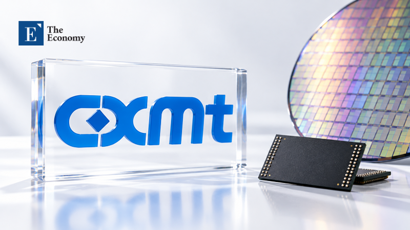
Chinese memory chipmaker ChangXin Memory Technologies (CXMT) is accelerating the development of next-generation memory cell structures. With restrictions limiting its access to extreme ultraviolet (EUV) lithography equipment from the Netherlands’ ASML, the company is overcoming some technological limitations by changing cell designs themselves to increase density. Market observers expect CXMT’s development of proprietary technology to accelerate further. It recently raised substantial research and development (R&D) funding through an initial public offering (IPO) and is building a stable domestic demand base by expanding supply agreements with major Chinese technology companies.
CXMT Announces Plans to Launch 4F² RDIMMs
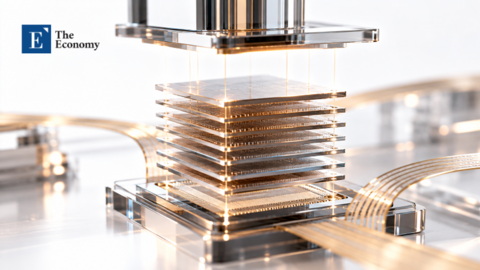
According to a report by technology news outlet Wccftech on the 10th (all dates hereafter are local time), CXMT President Cao Kangyu said at the fourth Integrated Circuits and Chiplets Conference held in Shanghai that day that the company would launch DDR5 RDIMM products using a 4F² memory cell architecture before the end of 2026. An RDIMM is a server memory module equipped with a register that relays command and address signals between the memory controller and DRAM chips to improve signal stability. The 4F² design reduces a cell’s footprint by changing the transistor’s current channel from a horizontal to a vertical orientation and placing a data-storage capacitor above it.
CXMT’s move is seen as an effort to overcome structural limitations facing China’s semiconductor industry. For decades, the DRAM industry has widely used a 6F² structure, in which transistors are arranged horizontally and each memory cell occupies an area equal to six times the square of the minimum feature size (F). Increasing density within this structure requires finer circuitry to reduce the area of individual cells. This is why major memory manufacturers, including Samsung Electronics, SK hynix and Micron, have aggressively adopted ASML’s EUV lithography equipment, which enables precise circuit patterns, as they compete to develop more advanced process nodes.
Why Was a 4F² Structure Needed?
Chinese companies, by contrast, face relatively significant constraints on scaling because U.S. export controls make it difficult to obtain ASML equipment. Finding alternative suppliers is also difficult, as ASML effectively holds a global monopoly on the production and supply of EUV lithography equipment. Against this backdrop, CXMT turned its attention to the 4F² structure. A 4F² structure can theoretically reduce the area of each cell by approximately 33% while retaining the same minimum feature size as the existing 6F² structure. Rather than using EUV equipment to draw more tightly packed circuits, it improves space utilization by changing the cell structure itself. It is considered a technological alternative that could allow CXMT to partially narrow the density gap with competitors that have EUV equipment while continuing to use its existing deep ultraviolet (DUV) equipment.
Since publishing its first research paper on a 4F² cell structure in 2021, CXMT has steadily continued developing related technologies and has recently been exploring the possibility of commercialization using existing DRAM manufacturing processes. Wccftech assessed that CXMT would likely begin by introducing some features of the 4F² structure based on its existing 15-nanometer-class G5 DRAM process. CXMT officially announced mass production using the G5 process in September. The process employs self-aligned quadruple patterning (SAQP), a technology that enables fine circuit patterns to be created using DUV lithography equipment.
IPO Strengthens Funding Base
Market observers expect CXMT’s technology development efforts to accelerate further. The substantial investment funds secured through its recent IPO support this outlook. According to Reuters, CXMT officially listed in July on the STAR Market, the Shanghai Stock Exchange’s board dedicated to technology companies. The offering price was CNY 8.66 per share (approximately USD 1.33), and the company issued approximately 6.68809 billion shares, raising CNY 57.92 billion (approximately USD 8.91 billion). This was the largest IPO ever by a mainland Chinese semiconductor company. Following the full exercise of the overallotment option, or greenshoe, the final number of shares issued rose to approximately 7.6913 billion, and total proceeds increased to CNY 66.607 billion (approximately USD 10.2 billion).
CXMT has said it will invest the funds raised in production process improvements and next-generation DRAM technology development. Specifically, a total of CNY 29.5 billion (approximately USD 4.54 billion) in IPO proceeds was allocated, including CNY 7.5 billion (approximately USD 1.15 billion) for technological upgrades to memory wafer mass-production lines, CNY 13 billion (approximately USD 2 billion) for advancing DRAM technology, and CNY 9 billion (approximately USD 1.38 billion) for R&D on next-generation DRAM technologies. In late September, the board also approved a plan to allocate CNY 13 billion of the excess proceeds to new technology R&D projects and CNY 5 billion (approximately USD 769 million) to the second phase of construction of a memory wafer back-end testing facility in Hefei.
Table 1. CXMT’s Progress in Securing Funding and Demand
| Category | Key Details |
|---|---|
| Securing Investment Funding | Total IPO proceeds of CNY 66.607 billion, with funds allocated to production line improvements, DRAM technology advancement, next-generation technology R&D, and back-end facility construction |
| Securing Customers | Signed a long-term supply agreement with Tencent and secured major Chinese technology companies, including Alibaba, ByteDance, Lenovo and Xiaomi, as customers |
Strong Domestic Demand in China
CXMT is also stepping up efforts to secure stable demand by signing large supply agreements with major Chinese technology companies. In June, Reuters reported that CXMT had signed a long-term server DRAM supply agreement worth more than CNY 20 billion (approximately USD 3.08 billion) with Chinese internet company Tencent. According to multiple people familiar with the matter, the contract runs for three to five years, while supply volumes and specific product specifications were not disclosed. Reuters reported at the time that CXMT was also discussing similar supply partnerships with other major Chinese internet companies.
Indeed, CXMT’s customer base has already expanded across China’s leading Big Tech companies. The securities filing submitted during CXMT’s IPO named Alibaba Cloud, ByteDance, Tencent, Lenovo, Xiaomi, Oppo and Vivo as major customers. As global memory manufacturers focused their resources on producing high-bandwidth memory (HBM) for artificial intelligence (AI) chips, supplies of conventional server DRAM tightened, prompting more Chinese companies to adopt domestically produced memory. This domestic demand base is expected to support CXMT’s capacity to invest in production facility expansion and next-generation process R&D.
Past Leaks of South Korean Process Information
Semiconductor process information previously leaked from South Korea is also highly likely to be serving as a springboard for CXMT. In January 2024, the Seoul Central District Prosecutors’ Office indicted and detained a former Samsung Electronics department head, identified by the surname Kim, on charges of stealing Samsung’s 18-nanometer DRAM process technology and using it to develop CXMT products. In May last year, prosecutors additionally indicted a former Samsung Electronics researcher, identified by the surname Jeon, on similar charges. According to prosecutors, Kim joined CXMT as head of development shortly after its establishment in 2016 with support from local Chinese governments. He led efforts to acquire related technologies by recruiting additional personnel from Samsung Electronics and South Korean semiconductor equipment companies. Jeon reportedly copied by hand and took out information covering hundreds of steps in Samsung Electronics’ DRAM process while moving to CXMT. Subsequent investigations also uncovered indications that SK hynix’s DRAM process technology had reached CXMT through a supplier employing former SK hynix personnel.
Prosecutors concluded that CXMT rapidly established its DRAM mass-production technology by using Samsung Electronics’ core process technology as its foundation and acquiring additional related technologies from other South Korean companies. They said CXMT’s developers modified and verified the leaked process information to suit production equipment in China and used it to become the first company in China to successfully mass-produce 10-nanometer-class DRAM in 2023. Courts have also repeatedly recognized that Samsung Electronics’ core technology was leaked to CXMT. Commenting on this, one market expert said, "Semiconductor suppliers’ data and know-how have astronomical value in their own right," explaining, "While some elements must of course be newly developed with each generation, a substantial portion builds on existing recipes." The expert added, "Acquiring a completed recipe can significantly reduce the time and cost of developing the next generation as well."
Aoife Brennan is a contributing writer for The Economy, with a focus on education, youth, and societal change. Based in Limerick, she holds a degree in political communication from Queen’s University Belfast. Aoife’s work draws connections between cultural narratives and public discourse in Europe and Asia.
Similar Post