China’s CXMT Achieves Just 25% HBM Yield as TSV and Bonding Barriers Thwart Near-Term Catch-Up

Anne-Marie Nicholson is a fearless reporter covering international markets and global economic shifts. With a background in international relations, she provides a nuanced perspective on trade policies, foreign investments, and macroeconomic developments. Quick-witted and always on the move, she delivers hard-hitting stories that connect the dots in an ever-changing global economy.
Authored On
Modified
U.S. export controls make HBM localization imperative for China’s AI industry
CXMT accumulates defects in large HBM dies and TSV processing
Technical burden mounts ahead of 12-Hi stacking and HBM3E entry
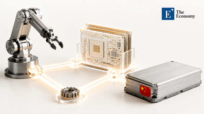
China’s largest DRAM manufacturer, ChangXin Memory Technologies (CXMT), has begun pilot production of fourth-generation high-bandwidth memory (HBM3), but its initial yields have struggled to improve. Although the company has built a relatively advanced production base for commodity DRAM, defects have compounded during the selection of large dies for HBM, through-silicon via (TSV) processing, and stacking and bonding. Mass production of fifth-generation HBM3E also requires process data accumulated through thermal and power management, integrated design, and customer validation, suggesting that investment alone will not be sufficient to overcome the technological hurdles.
Defect Rates Surge in Large HBM Dies
According to semiconductor industry sources on Sept. 14, the front-end yield—the proportion of functional units—for CXMT’s eight-layer HBM3 stacks, known as 8-Hi products, remains at approximately 30%. The yield is reportedly stuck at 25%, roughly one-third of the 80% threshold widely regarded as the “golden yield” benchmark for high-volume semiconductor manufacturing. Of the products that survive this stage, only about 70% ultimately qualify as functional units after back-end processing. In effect, for every 100 HBM3 products manufactured, only around 20 pass final testing, while nearly 80 are rejected as defective. CXMT is reportedly supplying these small batches of HBM samples to Chinese companies including Alibaba subsidiary T-Head and Cambricon as it continues working to improve yields.
The obstacle confronting CXMT lies not in its advanced DRAM process technology but in HBM manufacturing. A senior semiconductor equipment industry executive familiar with CXMT’s operations said, “There are no major problems with the commodity DRAM itself produced using CXMT’s ‘G4’ process, which is a 17-nanometer-class node used for HBM. However, DRAM dies used for HBM are larger than commodity products and subject to more demanding electrical specifications, making it considerably more difficult to meet qualification standards even when they are produced on the same process.” This suggests that CXMT’s underlying capabilities in commodity DRAM production have reached a relatively advanced level, but bottlenecks emerge when the company attempts to translate that foundation into high-performance HBM.
TSV Precision Impedes High-Layer Stacking
Industry observers identify the TSV process as the principal source of this bottleneck. TSVs are microscopic copper interconnects that vertically connect individual layers and transmit electrical signals when multiple DRAM dies are stacked, as in HBM. The highly complex process involves thinning a DRAM wafer to a thickness of only several dozen micrometers—a fraction of the width of a human hair—before drilling thousands of microscopic holes through the silicon and filling them completely with copper. A single misaligned hole or an incompletely filled copper via can render the entire layer defective, making TSV formation one of the most precision-intensive processes in semiconductor manufacturing.
This is precisely where the technological gap between CXMT and the industry leaders is widest. According to semiconductor research firm Nomad Semi, Samsung Electronics’ second-generation HBM2 contains more than 5,000 TSVs per die, while SK hynix’s HBM3 contains more than 8,000, compared with only around 3,000 for CXMT. Fewer TSVs indicate that CXMT has lowered process complexity at the expense of bandwidth—the volume of data processed per unit of time—yet its yields still remain far below those of Samsung Electronics and SK hynix. TSV formation is challenging even for the industry’s leading companies: SK hynix publicly disclosed that the yield for its standalone TSV process stood at only 40–60% in 2024.
Further yield losses occur during the back-end stacking and bonding stage, when the dies are physically assembled. If even one of the eight dies is misaligned, microscopic voids form at a bonding interface, or a layer warps during thermocompression bonding, the entire stack must be discarded. As the number of stacked layers increases, so does the number of potential defect points, causing process complexity to rise exponentially. With CXMT already constrained by low yields at the eight-layer stacking stage, the technological burden is expected to intensify further as the company transitions to products containing 12 or more layers.
Table 1. Core Processes Determining HBM Yields and CXMT’s Technological Limitations
| Category | Core Details | Technology and Yield Status | Principal Limitations |
|---|---|---|---|
| TSV Process | Thousands of microscopic holes are drilled into a thinned DRAM wafer and filled with copper to connect each layer vertically | Even a minor defect in hole alignment or copper filling can render the entire die defective | The most precision-intensive stage of HBM manufacturing |
| TSV Technology Gap | TSVs per die exceed 5,000 in Samsung Electronics’ HBM2 and 8,000 in SK hynix’s HBM3, compared with approximately 3,000 in CXMT’s products | CXMT has reduced the number of TSVs to lower process complexity, but its yields remain far below those of industry leaders | Lower bandwidth caused by fewer TSVs coincides with persistently low yields |
| Stacking and Bonding Process | A single instance of die misalignment, void formation at a bonding interface, or warpage during thermocompression bonding can render the entire stack defective | As the number of layers increases, potential defect points multiply and process complexity rises sharply | CXMT, already facing a yield bottleneck at eight layers, will encounter a heavier technological burden when transitioning to 12 or more layers |
Large-Scale Investment Continues Despite Weak Yields
Despite its low yields, China is unlikely to abandon HBM development. Localizing HBM production is directly tied to the survival of China’s artificial intelligence (AI) industry, which remains constrained by U.S. export controls. With Washington continuing to restrict exports of advanced AI semiconductors to China, domestically produced HBM is regarded as a critical foundation for sustaining the country’s AI chip ecosystem. According to Reuters, CXMT currently has monthly DRAM production capacity of 300,000 wafers across Hefei and Beijing, while also pursuing the construction of new fabs in Shanghai and Hefei and a second facility in Beijing. If investment proceeds as planned, monthly capacity could exceed 600,000 wafers. The prevailing assessment is that despite the substantial technology gap, the company has ample financial resources and manufacturing capacity to sustain repeated cycles of trial and error.
China’s advances have also begun to weigh on the pricing power of Samsung Electronics and SK hynix. Supply negotiations between Apple and CXMT are a prominent example. Apple tested CXMT’s LPDDR5X low-power DRAM for potential use in iPhones and MacBooks while also demanding lower prices during supply negotiations. The talks collapsed after CXMT insisted on prices comparable to or higher than those of Samsung Electronics and SK hynix, but Apple is reportedly continuing to validate its products. South Korean suppliers have benefited for now, but the moment CXMT entered Apple’s pool of prospective suppliers, Apple gained another lever with which to pressure its incumbent vendors. Industry observers believe that as shipments of Chinese-made DRAM increase, the ability of Samsung Electronics and SK hynix to defend their pricing could weaken.
CXMT’s HBM3E Challenge: Replicating Yields and Performance at Scale
For CXMT’s supply expansion to become a meaningful variable in HBM pricing, however, the company must advance from HBM3 samples to stable mass production of HBM3E or more advanced products. Because HBM3E delivers faster data-transfer speeds, it is subject to considerably tighter tolerances for power consumption, heat generation, and signal interference. Achieving target performance in a limited number of prototypes and maintaining consistent quality across an entire contracted volume are fundamentally different challenges. Customer approval for mass production will be possible only if CXMT can replicate its initial yields and performance after production volumes increase.
The first step toward improving yields is more rigorous screening before stacking. Experts broadly agree that CXMT must first upgrade its ability to accurately identify known good dies (KGDs) for stacking. Dies classified as functional during wafer-level testing may still develop latent defects under high-temperature and high-voltage conditions or during prolonged computation. If CXMT cannot trace the location and cause of defects at the die level, it will inevitably incur losses from discarding entire stacks that have already been assembled. A data infrastructure capable of immediately feeding test results back into front-end process parameters is likewise essential for stable mass production.
Thermal and Power Management Present Further Hurdles
Beginning with HBM3E, thermal performance and power efficiency become as critical as yield. As data-transfer speeds increase, more current flows through the TSVs and input/output circuitry, while even small differences in contact resistance can generate substantial heat across the entire stack. If heat becomes concentrated in a particular layer, signal errors can increase while DRAM operating speeds and service life deteriorate. Preventing this outcome requires coordinated optimization spanning low-voltage DRAM design, TSV layout, the base die’s power distribution network (PDN), and package-level thermal design. Incremental improvements to the DRAM process and back-end processing in isolation have clear limitations, making integrated design capabilities across both domains indispensable.
The next test for CXMT will be real-world AI accelerator validation of the samples supplied to Alibaba’s T-Head and Cambricon. Even after passing standalone memory testing, HBM must undergo further assessment of signal integrity and thermal characteristics within a GPU-oriented system-in-package (SiP), meaning that mass-production approval requires design refinements tailored to each customer’s specifications and additional validation. A quality-improvement system capable of rapidly incorporating signal errors, power fluctuations, and degradation observed under high-temperature, high-load conditions into product design and production lines will also be crucial to stabilizing yields. Manufacturing capacity and research headcount can be expanded through capital investment, but the data required to refine process parameters and stabilize yields can only be accumulated through repeated production runs and customer validation. Stabilizing the process so that electrical characteristics and yields remain consistent even during high-volume production of products built to the same specifications is a prerequisite for securing long-term supply contracts.
Anne-Marie Nicholson is a fearless reporter covering international markets and global economic shifts. With a background in international relations, she provides a nuanced perspective on trade policies, foreign investments, and macroeconomic developments. Quick-witted and always on the move, she delivers hard-hitting stories that connect the dots in an ever-changing global economy.
Similar Post