“Competition Is Already Fierce”: Japan’s Rapidus Faces Concerns Over Delayed 2nm Mass Production, With Returns on Massive Government Investment Uncertain

Aoife Brennan is a contributing writer for The Economy, with a focus on education, youth, and societal change. Based in Limerick, she holds a degree in political communication from Queen’s University Belfast. Aoife’s work draws connections between cultural narratives and public discourse in Europe and Asia.
Authored On
Modified
Japan’s Rapidus considers delaying 2nm semiconductor mass production after hitting technical barriers
Commercial viability remains uncertain despite massive Japanese government support, raising fears of a repeat of Elpida Memory’s fate
TSMC, Samsung Electronics and Intel accelerate advanced-process mass production and customer acquisition
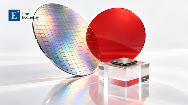
Japan’s state-backed foundry company Rapidus is considering postponing the start of mass production of advanced 2-nanometer (nm, one-billionth of a meter) semiconductors. Unresolved technical challenges required for mass production appear to be pushing the schedule behind its original plan. Market observers warn that if this scenario materializes, Rapidus could lose its footing in the already heated competition among 2nm foundries. With major foundry companies such as TSMC, Samsung Electronics and Intel accelerating the commercialization of next-generation processes and efforts to secure customers, they say the barriers to market entry for latecomers will inevitably grow over time.
Rapidus Struggles With 2nm Mass Production
On the 11th, Japan’s Jiji Press reported that Rapidus was considering postponing mass production of 2nm semiconductors from the second half of fiscal 2027 (October 2027–March 2028), as originally scheduled, to fiscal 2028 (April 2028–March 2029). Rapidus is a semiconductor company established in 2022 with investments from major Japanese companies including Toyota, Sony, NTT and SoftBank. It has been pursuing commercialization of a cutting-edge 2nm process through technical cooperation with IBM of the United States. In July last year, it announced that it had successfully fabricated prototype transistors, the core devices of the 2nm process, at its plant in Chitose, Hokkaido. However, it has reportedly since encountered setbacks in developing technology to connect individual devices and integrate them with other circuit components.
On the 10th, Bloomberg also reported that Rapidus had failed to achieve normal operation of static random-access memory (SRAM) cells, which temporarily store data inside a processor. According to the report, delays in developing key technologies originally due for completion by this summer had put the overall mass-production preparation schedule at least several months behind. Improving yield—the percentage of usable chips—and stabilizing production processes also remain challenges. Rapidus is currently facing persistent difficulties in raising yields and reportedly has yet to resolve issues with dust and fine-particle control in its cleanrooms, the facilities where semiconductors are manufactured.
TSMC Leads the Market
Against this backdrop, market observers warn that Rapidus’s position could become precarious amid intensifying 2nm competition. Taiwan’s TSMC is currently regarded as the market leader. TSMC began mass production using its 2nm (N2) process, which employs nanosheet transistors with a next-generation gate-all-around (GAA) architecture, in the fourth quarter of last year. This year, it has been rapidly increasing output, primarily at its Hsinchu and Kaohsiung facilities. In the third quarter of this year, the 2nm process’s share of total wafer revenue rose to 8%. To meet growing demand for smartphone, artificial intelligence (AI) and high-performance computing (HPC) chips in 2027, TSMC plans to more than double annual production capacity for its 2nm-family processes compared with this year.
Development of follow-on processes is also underway. TSMC plans to begin mass production in the second half of this year using its N2P process, which improves performance and power efficiency over the existing 2nm process, and its A16 process, which incorporates backside power delivery technology. N2P offers a performance improvement of approximately 5% over the existing N2 process, while A16 is designed to deliver 8–10% higher computing speeds than N2P or reduce power consumption by 15–20% at the same performance level. Meanwhile, the 1.4nm-class A14 process is scheduled to begin trial production in 2027 and full-scale mass production in 2028, with preparations to secure production capacity currently underway.
Samsung Electronics Also Races Ahead With Advanced Processes
Samsung Electronics is also accelerating its expansion of mass production as it improves yields on its 2nm process. According to a September analysis by Taiwanese market research firm TrendForce, Samsung Electronics’ 2nm GAA process yield, which was below 50% at the beginning of this year, has reportedly recently risen to around 70%. Building on this progress, Samsung Electronics plans to pursue mass production of mobile chips using its second-generation 2nm process (SF2P) in the second half of this year. During last month’s third-quarter earnings announcement, the company also offered an optimistic outlook, saying that 2nm orders were increasing, particularly from AI and HPC customers including major hyperscalers, and that the number of projects secured for its 2nm process this year would more than double from last year.
Efforts to expand production capacity in response to growing orders have also accelerated. Samsung Electronics is preparing to bring its Taylor plant in Texas into operation, anticipating that mass production of major customers’ new 2nm products will begin in earnest in the second half of next year. The Taylor plant has begun operating its cleanrooms and bringing in equipment, and wafer starts to establish production lines have also been confirmed to be underway. In addition, Samsung Electronics is reportedly continuing discussions on expanding its 2nm process, previously focused on mobile chips, into AI and HPC applications, while also preparing to develop experimental 1.4nm chips with multiple customers.
Table. Advanced-Process Development at Major Foundry Companies
| Company | Process | Key Details |
|---|---|---|
| TSMC | 2nm (N2) | Mass production began in the fourth quarter of last year; production capacity in 2027 is expected to more than double from this year |
| N2P·A16 | Mass production scheduled for the second half of this year; improved performance and power efficiency over the existing 2nm process | |
| 1.4nm (A14) | Trial production in 2027; full-scale mass production scheduled for 2028 | |
| Samsung Electronics | 2nm (SF2P) | Yield improved to approximately 70%; mobile chip mass production planned for the second half of this year |
| 1.4nm | Preparing to develop experimental chips with multiple customers | |
| Intel | 18A·18A-P | 18A production began last year; trial production of the performance-enhanced 18A-P began in June this year |
| 1.4nm (14A) | Trial production in the second half of 2027; mass production planned for 2028 |
2nm Competition Nears a Turning Point
U.S. chipmaker Intel also views 2027–2028 as a critical turning point for its advanced foundry business. After beginning production using its 1.8nm-class (18A) process last year, Intel started trial production of its performance-enhanced 18A-P process in June this year. Its next-generation 1.4nm-class 14A process is also scheduled for trial production in the second half of 2027, followed by full-scale mass production in 2028. Through these efforts, Intel aims to bring its foundry business to break-even by the end of 2027. However, in August, Intel Chief Financial Officer (CFO) David Zinsner explained that the break-even date could be pushed back to 2028 if securing customers creates additional investment requirements.
Related industries are also accelerating the development and commercialization of new products using 2nm processes. For example, South Korean AI chip company DeepX completed the design of its next-generation AI chip, the DX-M2, using Samsung Electronics’ second-generation 2nm process and completed tape-out early this month. The DX-M2 is designed to run generative AI in robots and industrial equipment using approximately 5 watts (W) of power. DeepX plans to obtain its first prototypes in March 2027 and begin supplying evaluation samples to customers in the second quarter of the same year. It then plans to begin initial mass production in the fourth quarter before moving into mass production in 2028.
Is Japan’s Semiconductor Comeback Blueprint Fading?
As 2nm competition in the global semiconductor market grows fiercer by the day, a delay in mass production risks dealing a devastating blow to Rapidus. Some observers even warn that the Japanese government’s massive support may fail to deliver meaningful results. In April, Japan’s Ministry of Economy, Trade and Industry decided to provide Rapidus with an additional JPY 631.5 billion in research and development funding, bringing cumulative support to JPY 2.354 trillion. Last month, a proposal was also put forward to invest an additional total of JPY 400 billion over fiscal 2027–2029 to strengthen Rapidus’s capital base. Yet not only is the timetable for mass production using its advanced process uncertain, but its efforts to secure customers also remain essentially at an early stage. On the 7th of last month, Reuters reported that Rapidus was pursuing cooperation with 17 companies, including Synopsys and Infosys, to support semiconductor design, but that it remained uncertain whether this would lead to actual large-scale contract manufacturing agreements.
There are also concerns that Rapidus could follow in the footsteps of Japanese DRAM maker Elpida Memory. Elpida was established in 1999 through the merger of NEC’s and Hitachi’s DRAM businesses. It grew into a major specialist DRAM manufacturer after acquiring Mitsubishi Electric’s DRAM business in 2003. However, following the global financial crisis in the late 2000s, its financial difficulties deepened as adverse factors mounted, including a sharp decline in semiconductor prices, intensifying competition with South Korean companies such as Samsung Electronics, and weaker export competitiveness due to a stronger yen. In 2009, the Japanese government invested JPY 30 billion in Elpida through the Development Bank of Japan and supported bank lending to the company. Ultimately, however, Elpida filed for court protection in February 2012 with approximately JPY 448 billion in debt and was acquired by U.S.-based Micron in 2013.
Aoife Brennan is a contributing writer for The Economy, with a focus on education, youth, and societal change. Based in Limerick, she holds a degree in political communication from Queen’s University Belfast. Aoife’s work draws connections between cultural narratives and public discourse in Europe and Asia.
Similar Post