"Breaking Through the Limits of Process Shrinkage" Advanced Packaging Reshapes the Semiconductor Competitive Landscape as TSMC-Led Backend Ecosystem Reorganization Accelerates

Aoife Brennan is a contributing writer for The Economy, with a focus on education, youth, and societal change. Based in Limerick, she holds a degree in political communication from Queen’s University Belfast. Aoife’s work draws connections between cultural narratives and public discourse in Europe and Asia.
Authored On
Modified
Advanced packaging emerges as a critical differentiator in semiconductor technology competitiveness
Foundry leader TSMC significantly expands investment in advanced packaging
Taiwan's backend semiconductor ecosystem increasingly aligns with TSMC, with capacity expansion gathering pace

Advanced packaging is rapidly emerging as a new competitive frontier in the global semiconductor industry. As conventional process scaling approaches its technological limits, packaging technologies that integrate multiple chips at high density to boost overall performance are becoming an equally critical determinant of competitiveness. Taiwan Semiconductor Manufacturing Co. (TSMC), the world's leading foundry, has been aggressively ramping up investment in advanced packaging to capitalize on this trend, while materials, equipment, and backend manufacturing suppliers are expanding production capacity in line with TSMC's capacity expansion plans and process standards.
The Rising Importance of Advanced Packaging Technology
According to industry sources on July 10, advanced packaging has recently emerged as one of the semiconductor industry's most important growth drivers. As conventional process scaling—long centered on shrinking circuit geometries to improve chip performance—runs into both technical and economic barriers, packaging, once viewed primarily as a means of protecting semiconductor chips, has evolved into a key enabler of continued performance gains. Market research firm Yole Group projects that the advanced packaging market will expand from USD 37.8 billion in 2023 to USD 69.5 billion by 2029. The market is expected to grow at a compound annual growth rate of 10.7% over the period.
The global artificial intelligence (AI) boom has further underscored the strategic importance of advanced packaging. Running large-scale AI models requires not only high-performance computing chips but also ultra-fast data transfers between graphics processing units (GPUs) and high-bandwidth memory (HBM). Even GPUs fabricated using cutting-edge process technologies can suffer from limited commercial competitiveness and constrained shipment volumes if bandwidth between GPUs and HBM is insufficient or packaging yields remain low. Technologies underpinning this architecture include 2.5D packaging, which integrates GPUs and HBM on a silicon interposer; 3D stacking, which vertically stacks memory chips; and chiplet and heterogeneous integration technologies that combine chips with different functions into a single package.
This trend has fundamentally altered the traditional investment paradigm that had long been dominated by outsourced semiconductor assembly and test (OSAT) companies. Major foundries are now making substantial investments in packaging themselves. SK hynix, for example, is constructing its P&T7 advanced packaging facility in the Cheongju Technopolis Industrial Complex to strengthen its packaging capabilities. The project carries an investment of approximately USD 13.8 billion, with completion targeted for the end of 2027. Samsung Electronics, meanwhile, is promoting a turnkey strategy that integrates foundry, memory, and packaging services. Through its I-Cube, H-Cube, and X-Cube 2.5D and 3D packaging platforms, Samsung integrates heterogeneous chips—including GPUs, central processing units (CPUs), and HBM—into a single package. Intel is likewise expanding its advanced packaging business based on high-density chiplet architectures through its proprietary EMIB and Foveros technologies.
TSMC Accelerates Packaging Investment
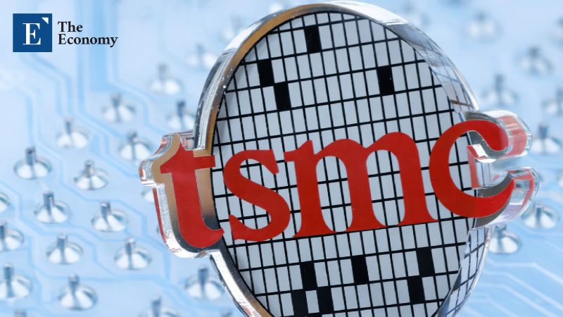
TSMC, the global leader in the foundry industry, is also pursuing aggressive investments in advanced packaging. The company has already established advanced packaging production bases across Taiwan, including Longtan in Taoyuan, Hsinchu Science Park, Zhunan in Miaoli County, Central Taiwan Science Park, and Southern Taiwan Science Park, while developing Chiayi Science Park as its next-generation backend manufacturing hub. According to the Taipei Times, TSMC plans to build two CoWoS (Chip-on-Wafer-on-Substrate) advanced packaging facilities at Chiayi Science Park, with the first plant scheduled for completion later this year. CoWoS is TSMC's proprietary 2.5D and 3D semiconductor packaging technology.
TSMC is also pursuing plans to construct two advanced packaging plants in Arizona and is currently undergoing the permitting process for the first facility. Last month, the company signed a 10-year strategic agreement with U.S.-based packaging and testing company Amkor Technology to deepen cooperation in advanced packaging. Through the partnership, TSMC plans to expand packaging capacity in Arizona while accelerating investment across the U.S. semiconductor supply chain ecosystem. Commenting on the agreement, Amkor CEO Kevin Engel stated, "This collaboration will allow us to provide customers with a comprehensive local supply chain spanning advanced wafer fabrication, packaging, and testing."
TSMC's next-generation CoPoS (Chip-on-Panel-on-Substrate) packaging technology, developed to overcome the size limitations of conventional silicon interposers, is also attracting growing industry attention. In its recent Asia-Pacific Technology Industry report, Morgan Stanley projected that mass production of CoPoS could begin as early as 2028, ahead of previous expectations. The report cited the increasing size of AI chips and the growing market traction of Intel's competing EMIB-T technology as factors driving the accelerated commercialization timeline. GPUs manufactured on sub-2-nanometer process technologies and AI application-specific integrated circuits (ASICs) are considered among the most likely initial adopters.
Taiwan's Backend Semiconductor Ecosystem Expands Rapidly
TSMC's aggressive push into advanced packaging is reshaping the broader semiconductor ecosystem. Taiwan, home to TSMC, is increasingly becoming the global center of the advanced packaging supply chain. Japanese diversified chemicals company Asahi Kasei, for example, plans to expand processing capacity in Taiwan for Sunfort, its photosensitive film used in semiconductor package substrates. As booming AI semiconductor demand drives larger and more complex multilayer package substrates, the company aims to strengthen production capabilities to respond more quickly to major local customers such as TSMC. The expansion will involve the construction of a new manufacturing facility in Taiwan, with an investment totaling approximately USD 13.7 million.
OSAT providers are also accelerating their expansion efforts. TSMC has recently begun outsourcing production of relatively less complex redistribution layer (RDL) products to OSAT companies, as its internal CoWoS production capacity alone cannot satisfy surging AI and high-performance computing demand. In response, leading Taiwanese OSAT companies, including Powertech Technology Inc. (PTI) and ASE Technology Holding, are expanding production lines to meet TSMC's process and quality standards. ASE, in particular, is expected to increase its CoWoS production capacity to between 20,000 and 25,000 wafers per month by the end of this year. Package substrate manufacturers are also accelerating investment in line with the TSMC-centered ecosystem. Taiwan-based substrate supplier Kinsus is reportedly pursuing a long-term expansion strategy that calls for constructing new manufacturing facilities every two to three years.
Equipment suppliers are likewise benefiting from the investment wave. TSMC has partnered with ASE to establish the 3D IC Advanced Manufacturing Alliance, aimed at building a localized advanced packaging equipment supply chain. The alliance brings together backend process, equipment, materials, and inspection companies required for the mass production of 3D integrated circuits and advanced packaging technologies. A total of 37 companies—including Chroma ATE, Grand Process Technology, and Scientech Manufacturing—have joined the initiative. Together, they will align bonding, cleaning, inspection, heat treatment, and other advanced packaging processes with TSMC's manufacturing standards while improving production yields and ensuring stable equipment supplies.
Aoife Brennan is a contributing writer for The Economy, with a focus on education, youth, and societal change. Based in Limerick, she holds a degree in political communication from Queen’s University Belfast. Aoife’s work draws connections between cultural narratives and public discourse in Europe and Asia.
Similar Post