“NVIDIA Alone Is Not Enough”: From Samsung-Backed Euclyd to Startups and Big Tech, Global AI Chip Race Intensifies

Oliver Griffin is a policy and tech reporter at The Economy, focusing on the intersection of artificial intelligence, government regulation, and macroeconomic strategy. Based in Dublin, Oliver has reported extensively on European Union policy shifts and their ripple effects across global markets. Prior to joining The Economy, he covered technology policy for an international think tank, producing research cited by major institutions, including the OECD and IMF. Oliver studied political economy at Trinity College Dublin and later completed a master’s in data journalism at Columbia University. His reporting blends field interviews with rigorous statistical analysis, offering readers a nuanced understanding of how policy decisions shape industries and everyday lives. Beyond his newsroom work, Oliver contributes op-eds on ethics in AI and has been a guest commentator on BBC World and CNBC Europe.
Authored On
Modified
Samsung Electronics Co-Leads Euclyd’s Series A Funding Round
Euclyd Targets Inference Efficiency Through Processor-Memory Co-Design
AI Chip Competition Intensifies, Raising Questions Over the End of NVIDIA’s Monopoly Era
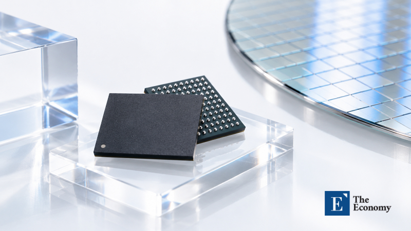
Samsung Electronics has invested in Dutch artificial intelligence (AI) semiconductor startup Euclyd. As power consumption and memory bottlenecks at AI data centers become increasingly severe, Samsung aims to use Euclyd’s processor-memory co-design technology to position itself ahead of changes in the next-generation AI infrastructure market. With Euclyd and numerous other companies accelerating the development of proprietary AI chips, analysts increasingly expect the established competitive order centered on NVIDIA to come under pressure.
Euclyd Secures Series A Funding
According to semiconductor industry sources on September 21, Euclyd announced on September 15 (all dates local) that it had secured more than $231 million in Series A funding. The round was co-led by Samsung Catalyst Fund, Samsung Electronics’ corporate venture capital (CVC) arm; Dutch investment firm Somerset Capital Partners; the EQT-managed Scaleup Europe Fund; and European deep-tech venture capital (VC) firm Innovation Industries. Other participants included the Export and Investment Fund of Denmark (EIFO), Denmark’s state-backed investment institution; semiconductor-focused VC firm imec.xpand; and the Brabant Development Agency (BOM) of the Netherlands. The company did not disclose its post-investment valuation or the amount contributed by each investor.
Euclyd is a semiconductor startup founded in the Netherlands in 2024, with its name derived from the ancient Greek mathematician Euclid. The company aspires to redesign AI chips from “first principles,” rather than developing them merely as extensions of existing products. Samsung Electronics’ investment in Euclyd was likewise motivated by the efficiency and scalability offered by its technology, which could address the limitations of existing AI infrastructure. “The next phase of AI will be defined not only by model innovation, but also by the efficiency and scalability of its infrastructure,” said Dede Goldschmidt, head of the Samsung Semiconductor Innovation Center at Samsung Electronics. “Euclyd combines an accomplished team with a differentiated vision for addressing constraints in AI data centers.”
Potential for Greater AI Infrastructure Efficiency
Euclyd’s vision focuses on the inference stage of AI models. In general, as the adoption of generative AI and agentic AI expands, the volume of inference computations required to run the same model repeatedly increases rapidly, driving corresponding growth in data center power consumption, memory bandwidth requirements and infrastructure buildout costs. Euclyd believes that the so-called “memory wall”—where memory’s ability to supply data fails to keep pace with improvements in processor performance, constraining the entire system—has emerged as a critical obstacle to the expansion of AI infrastructure.
Euclyd’s core strategy for overcoming these limitations is “processor-memory co-design.” Unlike the conventional approach of developing processors and memory separately before connecting them, processor-memory co-design builds the two components as a single system from the outset. Rather than indiscriminately increasing the processing speed of computing devices alone, the approach jointly optimizes memory architecture and data-transfer pathways to deliver the data required for computation as quickly as possible, thereby reducing both latency and power consumption.
Lower Costs Through Proprietary Technology
The principal products incorporating this design are “craftwerk,” an AI inference chip, and “craftwerk station (CWS),” a rack-scale data center system equipped with the chip. Craftwerk uses programmable application-specific integrated circuit (ASIC) compute to operate multiple dedicated processing units in parallel, combining them with Euclyd’s proprietary memory architecture and system-level optimization technology. Based on its own simulations, Euclyd claims that this architecture can deliver greater power efficiency than existing high-performance AI systems in certain large language model (LLM) inference environments while substantially reducing the cost per token.
Euclyd has devised two principal business models around the technology. The first is to supply chips and rack systems directly to companies seeking to operate AI models in their own facilities for security and other reasons. The second is to provide processor- and memory-related intellectual property (IP) to companies developing proprietary AI chips. In an interview with CNBC, Euclyd Chief Executive Officer (CEO) Bernardo Kastrup outlined a goal of “beginning the full-scale rollout of physical semiconductor systems in 2028 and securing thousands of enterprise customers by 2030.” However, because Euclyd is still an early-stage company founded in 2024, it has yet to establish a track record of validating its systems under development in large-scale commercial environments.
AI Chip Market Heats Up
Beyond Euclyd, a growing number of companies have recently entered the AI chip market in an effort to disrupt the established competitive order dominated by NVIDIA. Prominent examples include U.S.-based d-Matrix and Tenstorrent. D-Matrix, which develops AI inference chips, raised $275 million in Series C funding last November at a valuation of $2 billion and began full-scale production of its proprietary Corsair inference accelerator in June this year. Tenstorrent also began commercial shipments of its Galaxy Blackhole AI acceleration system in April. Galaxy Blackhole integrates compute, memory and networking into a single system designed to handle workloads including LLM inference and image generation.
U.S.-based Cerebras Systems is also expanding rapidly on the strength of its proprietary architecture. Rather than cutting a wafer into hundreds of individual chips, as conventional semiconductor manufacturing does, Cerebras developed the “Wafer Scale Engine (WSE),” which uses an entire wafer as a single large processor. The company secured a valuation of $6.4 billion when it listed on Nasdaq in May this year, while its operational or secured data center capacity exceeded 600 megawatts (MW) as of the second quarter. More recently, it has accelerated the joint development of AI infrastructure with AMD by combining Cerebras’ low-latency inference systems with AMD graphics processing units (GPUs).
Table 1. Proprietary AI Chip Development at Major Companies
| Company | Proprietary Chip/System | Development and Commercialization Status |
|---|---|---|
| Euclyd | craftwerk·craftwerk station | Developing a processor-memory co-design inference system, targeting a 2028 launch |
| d-Matrix | Corsair | AI inference-optimized accelerator, entered full-scale production in June this year |
| Tenstorrent | Galaxy Blackhole | Integrated compute, memory and networking AI system, commercial shipments began in April this year |
| Cerebras Systems | Wafer Scale Engine | Uses an entire wafer as a single processor, developing infrastructure integrating AMD GPUs |
| AMD | Instinct MI400·Helios | Unveiled a rack-scale system connecting 72 GPUs, pursuing supply agreements with OpenAI and Anthropic |
| Huawei | Ascend·SuperPoD | Building an integrated chip, server and networking ecosystem, accelerating the Ascend 960DT launch schedule |
| Amazon Web Services | Trainium | Deploying 3-nanometer-based Trainium3 in services, supporting Anthropic’s training and inference workloads |
| Microsoft | Maia 200 | Developing a proprietary inference accelerator for Azure, Copilot and OpenAI models |
| Tensor Processing Unit | Developed seven generations through Ironwood, establishing a large-scale cloud interconnection architecture | |
| OpenAI | Jalapeño | Inference ASIC jointly developed with Broadcom, scheduled for data center deployment at the end of this year |
Big Tech Enters the Fray
Beyond collaborating with other companies, AMD is also working to strengthen its proprietary competitiveness. In July, it unveiled its next-generation Instinct MI400-series GPUs and Helios, a rack-scale system capable of connecting as many as 72 GPUs. OpenAI plans to begin using Helios in the fourth quarter of this year, while Anthropic has agreed to deploy as much as 2 gigawatts (GW) of MI450-series GPUs beginning next year. In China, Huawei is aggressively expanding its proprietary AI semiconductor ecosystem. Centered on its Ascend-series accelerators, Huawei is simultaneously developing chips, servers and networking technology while pursuing a strategy to improve the performance of large-scale AI systems through products such as SuperPoD, which connects thousands of chips. On September 17, the company also moved the launch of its next-generation Ascend 960DT forward from its original schedule to the first quarter of 2027.
Major cloud providers are likewise moving rapidly to bring AI chip development in-house. Amazon Web Services (AWS) continues to enhance its proprietary Trainium AI accelerator. The 3-nanometer-based Trainium3 is currently being deployed in commercial services, while Anthropic is using more than 1 million Trainium2 chips to train and run inference for Claude. Microsoft (MS) also unveiled its proprietary Maia 200 inference accelerator in January and announced plans to deploy it to run Azure, Microsoft Foundry, Copilot and OpenAI’s GPT-family models. Google began developing its proprietary Tensor Processing Unit (TPU) AI accelerator approximately a decade earlier. Its latest product is the seventh-generation Ironwood TPU, which can reportedly connect as many as 9,216 chips within a single pod. More recently, OpenAI has also entered the chip design race. In June, OpenAI unveiled Jalapeño, its first proprietary AI accelerator jointly developed with Broadcom. Jalapeño is an ASIC optimized for LLM inference and is scheduled to be deployed in data centers beginning at the end of this year.
Oliver Griffin is a policy and tech reporter at The Economy, focusing on the intersection of artificial intelligence, government regulation, and macroeconomic strategy. Based in Dublin, Oliver has reported extensively on European Union policy shifts and their ripple effects across global markets. Prior to joining The Economy, he covered technology policy for an international think tank, producing research cited by major institutions, including the OECD and IMF. Oliver studied political economy at Trinity College Dublin and later completed a master’s in data journalism at Columbia University. His reporting blends field interviews with rigorous statistical analysis, offering readers a nuanced understanding of how policy decisions shape industries and everyday lives. Beyond his newsroom work, Oliver contributes op-eds on ethics in AI and has been a guest commentator on BBC World and CNBC Europe.
Similar Post