“Riding the AI Demand Boom” TSMC Dominates Global Foundry and Packaging Markets, Accelerates Ecosystem Expansion with Japanese Materials, Components and Equipment Suppliers

Aoife Brennan is a contributing writer for The Economy, with a focus on education, youth, and societal change. Based in Limerick, she holds a degree in political communication from Queen’s University Belfast. Aoife’s work draws connections between cultural narratives and public discourse in Europe and Asia.
Authored On
Modified
Intensifying AI chip competition delivers clear gains for TSMC
TSMC’s robust packaging capabilities drive continued investment growth
TSMC deepens collaboration with technologically advanced Japanese materials and equipment suppliers
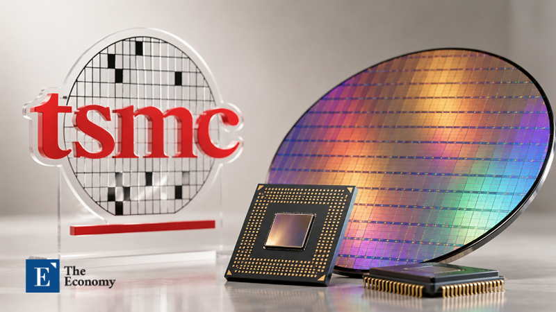
Taiwan’s TSMC is expected to emerge as the biggest beneficiary of the artificial intelligence (AI) semiconductor race. Demand for foundry orders from major fabless chipmakers, including Nvidia and AMD, is reinforcing TSMC’s market position, according to industry analysis. Its formidable back-end capabilities are also cited as a key competitive advantage. Having established proprietary advanced packaging technologies and secured a leading position in the market, TSMC is accelerating both capital investment and collaboration with Japanese semiconductor materials, components and equipment suppliers.
TSMC Rides the AI Boom
On August 31, U.S. investment publication The Motley Fool said, “Regardless of who wins the AI accelerator race, TSMC is likely to benefit structurally.” Nvidia and AMD, which currently lead the AI accelerator market, are fabless companies that design chips and outsource their production to foundries. As the world’s largest foundry and a leader in cutting-edge process technology, TSMC serves as a core manufacturing partner for both companies. According to The Motley Fool’s own research, TSMC accounted for approximately 72% of global foundry revenue as of the end of last year and is one of only a handful of companies capable of handling the massive volumes of advanced semiconductors required by Nvidia and AMD. This means that neither Nvidia nor AMD is likely to reduce its reliance on TSMC significantly in the near term.
TSMC is similarly optimistic about AI-driven demand. During the company’s second-quarter earnings conference call, TSMC Chairman and CEO C.C. Wei said, “We believe demand will be very strong from now through probably 2029 or 2030,” adding, “We cannot be certain whether there will be a temporary slowdown in between, but the underlying trend is very strong.” He said, “We are witnessing the emergence of a new industry that can be called the ‘AI industry,’” emphasizing that AI will affect virtually every sector, including automobiles and humanoid robots. Pointing to the vast amounts of capital being invested in AI, particularly by cloud service providers (CSPs), he stressed, “That alone makes it a highly significant new industry worldwide.” Wei expressed confidence that semiconductor chips lie at the foundation of this demand and that most of those chips are manufactured by TSMC.
Packaging Competitiveness Comes to the Fore
The market has recently begun to view advanced packaging as a new growth engine for the semiconductor industry. As the conventional race to improve performance by shrinking circuit linewidths encounters technological and economic limits, packaging—once regarded primarily as a means of protecting chips—has become a critical enabler of continued miniaturization. The global AI boom has further underscored the importance of advanced packaging. Running large-scale AI models requires not only high-performance compute chips but also rapid data exchange between graphics processing units (GPUs) and high-bandwidth memory (HBM). Even a GPU fabricated using the most advanced process node will inevitably face constraints on actual supply and product competitiveness if its interconnect bandwidth with HBM is insufficient or its packaging yield is low. The technologies underpinning this architecture include 2.5D packaging, which places GPUs and HBM together on a silicon interposer; 3D stacking, which vertically stacks memory chips; and chiplet and heterogeneous integration technologies, which combine chips with different functions.
TSMC’s flagship technology in this field is Chip-on-Wafer-on-Substrate (CoWoS). CoWoS is an advanced packaging technology that places GPUs or AI accelerators and multiple HBM stacks within a single large package and connects them at high speed. It is widely used by Nvidia and other major AI semiconductor companies. The latest CoWoS-L, in particular, uses local silicon interconnects (LSIs) only where needed instead of a large silicon interposer, enabling an even larger package footprint. Production stability has also reached a high level. TSMC said it achieved a yield of more than 98% this year for ultra-large CoWoS packages measuring 5.5 reticles. A reticle refers to the basic area over which lithography equipment can pattern circuitry in a single exposure.
Capital Investment Expansion
System on Integrated Chips (SoIC), a three-dimensional stacking technology, is another area of strength for TSMC. SoIC vertically stacks and connects chips with different functions, integrating logic chips, cache and input/output dies—each manufactured using its optimal process—as though they were a single semiconductor. TSMC is also strengthening its ability to validate the reliability of complete packaging systems. Beyond testing individual packages, the company is extending validation to the PCB, server and rack levels while shortening the development and qualification cycle for 3D-stacked products to approximately one year, allowing it to respond proactively to the rapid generational turnover of AI accelerators.
The scale of related investment is also expanding. TSMC has established advanced packaging production bases across several locations in Taiwan, including Longtan in Taoyuan, Hsinchu Science Park, Zhunan in Miaoli, Central Taiwan Science Park and Southern Taiwan Science Park. It is also developing Chiayi Science Park in southwestern Taiwan into a next-generation back-end manufacturing hub. According to the Taipei Times, two TSMC CoWoS advanced packaging plants are slated to be built at Chiayi Science Park, with the first facility targeted for completion this year. In addition, TSMC is pursuing plans to build two advanced packaging plants in Arizona and is currently proceeding with the permitting process for construction of the first facility. Last month, it also signed a 10-year agreement with U.S. outsourced semiconductor assembly and test (OSAT) provider Amkor Technology to strengthen cooperation in advanced packaging. Through the agreement with Amkor, TSMC intends to expand its packaging facilities in Arizona and accelerate investment in the semiconductor supply chain ecosystem.
Japanese Materials, Components and Equipment Suppliers Accelerate Expansion into Taiwan
The global packaging ecosystem is also being reorganized around Taiwan, TSMC’s home market. Japanese advanced packaging materials, components and equipment companies, in particular, are strengthening their production and customer support systems in Taiwan while tightening their supply chain ties with TSMC. One prominent example is Namics, a Japanese electronic materials supplier for semiconductor packaging. Namics primarily manufactures underfill materials that fill microscopic gaps between semiconductor chips and substrates to protect bonded interfaces, and operates a local production plant at Tongluo Science Park in Miaoli County, Taiwan. The plant produces chip underfill for semiconductor packaging and underfill for display driver chips. In October last year, Namics also opened a separate office in Hsinchu, where TSMC is headquartered, to strengthen its sales and technical support capabilities.
Japanese diversified materials and imaging company Fujifilm, meanwhile, is establishing its largest semiconductor materials production base in Taiwan in Hsinchu, with operations scheduled to begin in December. The facility will manufacture chemical mechanical polishing (CMP) slurry for advanced semiconductors and cleaning solutions used after the CMP process, while also performing research and development (R&D), quality evaluation, warehousing and logistics functions. The facility’s design reflects Fujifilm’s plan to establish a “local production, local consumption and local support” system centered on the new Hsinchu plant.
Table 1. Cooperation between Japanese Materials, Components and Equipment Suppliers and TSMC
| Company or Institution | Major Location | Initiative |
|---|---|---|
| Namics | Miaoli and Hsinchu, Taiwan | Local production of underfill for semiconductor packaging; stronger sales and technical support through its Hsinchu office |
| Fujifilm | Hsinchu, Taiwan | Establishment of an integrated local hub encompassing product manufacturing, R&D, quality evaluation and logistics |
| TSMC | Tsukuba, Japan | Joint development of advanced packaging materials, substrates and equipment technologies with approximately 120 Japanese companies |
| Japanese electroplating materials supplier | Taiwan | Establishment of a local production system with support from TSMC for production lines and quality inspection; shortened delivery lead times |
TSMC Also Steps Up Cooperation
TSMC is also actively pursuing cooperation with Japanese companies. It operates a 3D stacking R&D center in Tsukuba, Ibaraki Prefecture, where it jointly develops next-generation advanced packaging technologies with Japanese materials, components and equipment suppliers. Approximately 120 Japanese companies currently collaborate with the center, with research spanning the entire back-end process, from underfill, molding compounds and thermal interface materials (TIMs) to package substrates and process and inspection equipment. TSMC has also begun directly assisting Japanese suppliers with localization in Taiwan. TSMC said that this year it supported an unnamed Japanese supplier of electroplating additives for advanced packaging in establishing a plant in Taiwan, assisting with production line construction, equipment optimization, quality inspection and sample validation. As a result, additives previously imported from Japan are now produced directly in Taiwan, reducing the time required for production and supply from 60 days to 20 days.
TSMC’s expanding ties with Japan are underpinned by the country’s robust technological capabilities. Japanese materials, components and equipment suppliers have demonstrated outstanding R&D achievements not only in semiconductors but across a wide range of industries. A prominent example is Asahi Kasei, a Japanese diversified chemical company. Asahi Kasei recently developed an electrolyte-additive doping technology designed to prevent initial capacity loss in high-voltage batteries using silicon anodes. During initial charging, silicon anodes consume large quantities of lithium ions as a solid electrolyte interphase (SEI) layer forms on their surface, reducing the battery’s total energy density and shortening its service life. To address this problem, the researchers formulated a specialized additive using low-cost lithium carbonate, a widely used battery raw material, and devised a structure in which a small amount is introduced into the cathode to serve as a sacrificial lithium source during the first charge. In internal testing, cells incorporating the technology exhibited longer charge-discharge cycle life while maintaining a low cost per watt-hour (Wh). Asahi Kasei plans to conduct demonstration evaluations with global customers before pursuing commercialization through technology licensing.
Aoife Brennan is a contributing writer for The Economy, with a focus on education, youth, and societal change. Based in Limerick, she holds a degree in political communication from Queen’s University Belfast. Aoife’s work draws connections between cultural narratives and public discourse in Europe and Asia.
Similar Post